01 · Electron-transport layer screening
Two layers reach the absorber's current limit. Two collapse to nothing.
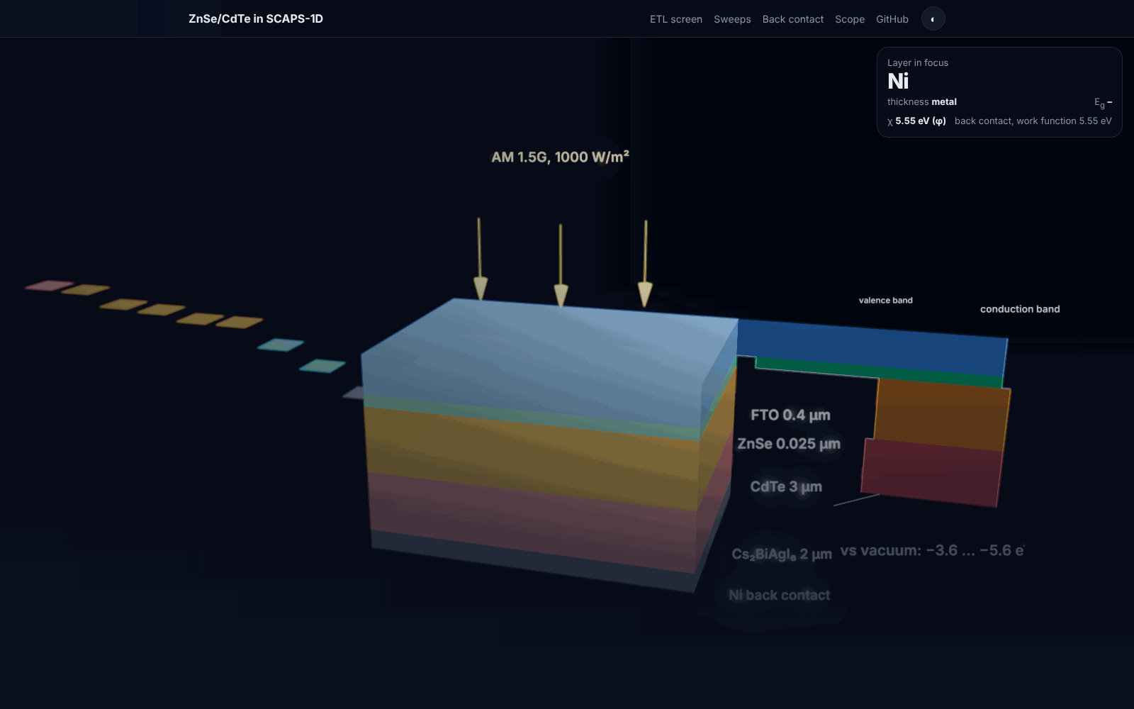
Each ETL was swept from 0.4 to 2.0 µm with the rest of the stack fixed (FTO 0.4 / ZnSe 0.025 / CdTe 3 µm / Ni). Cs₂BiAgI₆ and C₆₀ share near-ideal fill factors and almost the full 26 mA/cm² a 1.5 eV absorber can deliver under AM 1.5G; both have the same electron affinity as CdTe, so there is no conduction-band step. PCBM and WS₂ keep a normal VOC and fill factor but lose the current, so the loss is in collection, not the junction.
The stack, exploded, with its band alignmentFTOZnSeCdTeCs₂BiAgI₆Ni
Ten electron-transport layersbestabove 20 %5 to 20 %JSC
| ETL | t (µm) | VOC (V) | JSC | FF (%) | PCE (%) |
|---|
J-V curves at the best thickness, all tenribbons stacked by rank
02 · Layer thickness and temperature
The absorber gains current with thickness, the front contact loses it, the buffer is inert.
With Cs₂BiAgI₆ selected, each layer was swept in turn. Step through the sweeps: the J-V curve and the four metrics come straight from the SCAPS export for that point.
CdTe absorber
thickness sweep, 0.4 to 2.0 µm
–VOC (V)
–JSC (mA/cm²)
–FF (%)
–PCE (%)
CdTe absorber: 27.23 → 27.85 %
JSC rises with thickness as more photons are absorbed; VOC falls slightly with more bulk recombination. The optimum stack uses 3 µm.
FTO front contact: 27.89 → 26.96 %
Thinner is better. A thicker transparent conductor is a parasitic absorber in front of the junction.
ZnSe buffer: flat at 27.8 %
Performance moves by 0.02 points across 0.4 to 2.0 µm. The 2.9 eV window passes the spectrum to the absorber whatever its thickness; 0.025 µm is used.
Cs₂BiAgI₆ ETL: 27.81 → 27.99 %
A 0.18-point rise across the sweep; 2 µm is the end of the swept range.
Temperature: 300 → 400 K
JSC does not move. VOC falls at −1.66 mV/K as the dark saturation current rises, and efficiency derates at −0.049 points per kelvin, about −0.18 %/K relative, milder than crystalline silicon's −0.35 to −0.45 %/K.
J-V from 300 to 400 K300 K400 K
04 · Scope, and beyond the simulation
A screen of ten layers and nine metals, and the hardware it led to.
Scope and assumptionsSCAPS-1D is a one-dimensional planar drift-diffusion model with literature input parameters, so the study's product is the ranking of ten electron-transport layers and nine metals for a ZnSe/CdTe junction, the thickness trade-offs of each layer and the temperature derating of the optimum stack; 27.99 % is the simulated ceiling for this parameter set, and Cs₂BiAgI₆ as an ETL on CdTe is the experiment the study motivates.
Beyond the simulationThe project's hardware concept, a detachable spiral thin-film panel with 17.9 % more active area than a planar panel of the same footprint, holds two granted Indian design registrations (434427-001, October 2024; 459195-001, May 2025) with one utility application under review. The work received the Best Poster Award at the 61st Annual Convention of Chemists (ACC 2024).
git clone https://github.com/Soham-ChemE/Perovskite-Solar-Cell-SCAPS1D-Optimization.git
cd Perovskite-Solar-Cell-SCAPS1D-Optimization
pip install -r requirements.txt
./reproduce.sh    # figures, data/scaps_metrics.json and this page from the raw SCAPS exports
CiteS. Kavathekar, S. Malokar and S. Nagaraj, Optimisation of a ZnSe/CdTe thin-film solar cell with screened electron-transport layers and back contacts in SCAPS-1D, B.Tech capstone, Vellore Institute of Technology, 2025 (guide: Dr. Dharmendra Kumar Bal). github.com/Soham-ChemE/Perovskite-Solar-Cell-SCAPS1D-Optimization